
In 2020, photonics researchers used the finite element method (FEM) to make a number of exciting discoveries in the field of optics.
As discussed in a previous post, FEM is a numerical solution that breaks down a much larger, complex problem into a series of smaller ones (“finite elements”) in order to make the overall problem easier to examine. This equation is then used to create a digital simulation (known as the finite element analysis), which gives engineers a more detailed look into the design and how its various elements work together.
Last January, researchers used FEM to analyze topologically protected four-wave mixing (FWM) interactions in a plasmonic metasurface made up of intermittent arrangements of nanoholes in a graphene sheet.
“These findings could pave a new way for developing ultralow-power-consumption, highly integrated, and robust active photonic systems at deep-subwavelength scale for applications in quantum communications and information processing,” the researchers wrote in Science Advances.
That same month, a group of optics researchers used a 2-D FEM simulation that may lead to advancements in surface-emitting semiconductor lasers. These lasers are used in sensing, data communications, augmented reality glasses, and FaceID. Their research sheds light on a new way to create low-threshold, surface-emitting laser diodes that span between the ultraviolet to deep visible range.
“Our studies open a new paradigm for developing low-threshold surface-emitting laser diodes from the ultraviolet to the deep visible (~200 to 600 nm), wherein the device performance is no longer limited by the lack of high-quality [distributed Bragg reflectors] DBRs, large lattice mismatch, and substrate availability,” the authors wrote in Science Advances.
Low-threshold, highly efficient, all-epitaxial surface emitting green laser diodes can pave the way for a number of useful applications in the future. These include projection displays such as pico projectors, smart lighting, wireless communication, plastic optical fiber communication, biosensors, and optical storage.
In July, we reported on how scientists are using FEM to improve optical lenses, which are commonly found in electronic devices like cell phones and laptops, as well as in high-powered lasers used to create package labeling. Once thought impossible, researchers can now create “full-wave” simulations using FEM for optical wave analysis. The simulation solves the entire domain of what’s known as “Maxwell’s equations,” a complex set of equations that describe how electric charges and electric currents produce electric and magnetic fields. The simulation breaks everything down into a mesh and subdivides all elements into simpler shapes. Thanks to full-wave FEM analysis, scientists are much closer now to simulating whole optical systems.
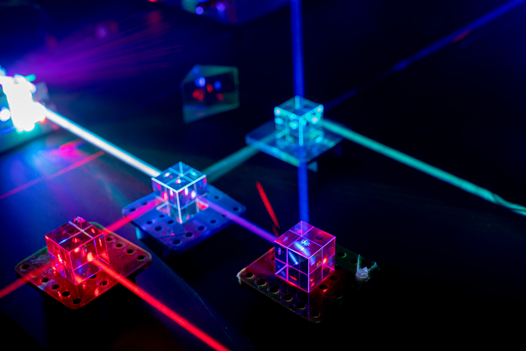
In the same month, researchers from Pennsylvania State University revealed how metasurfaces with unparalleled controllability of light may be able to transform traditional optics. “Metasurfaces” are thin, two-dimensional metamaterial layers that permit or prevent the propagation of electromagnetic waves in desired directions. They used FEM simulations to demonstrate a feasible way to control light on integrated photonics and free-space metasurfaces. This could mean that scientists will one day be able to make multifunctional photonic integrated devices with the ability to easily access free space, allowing for a range of advancements in optical communications.
“We have experimentally demonstrated off-chip beam deflection and focusing using the guided wave driven metasurfaces on silicon waveguides. In addition, two-dimensional (2D) manipulation of free-space light can be realized by placing a 2D array of meta-atoms on a slab waveguide. This technology can enable a wide spectrum of applications ranging from optical communications to LiDAR, as well as miniaturized display technology for virtual reality and augmented reality devices,” the researchers wrote in Science Advances.
In August, Chinese researchers from the Design and Simulation Technology Department at Focuslight Technologies used digital simulations, including FEM, to evaluate the thermal performance of high-power diode-lasers. That same month, researchers from the University of Rochester used FEM to test the smallest electro-optical modulator ever created, which they believe can some day serve as a platform for light-based photonics integrated circuits.
Given the number of breakthroughs FEM helped photonics researchers make in 2020, there’s a good chance it will lead to more in the new year.
Understand Finite Element Method for Photonics
Learn how FEM can be used to model and simulate photonic components/devices and analyze how they will behave in response to various outside influences. The Finite Element Method for Photonics course program provides a comprehensive and up-to-date account of FEM in photonics devices, with an emphasis on practical, problem-solving applications and real-world examples. Engineers will gain an understanding of how mathematical concepts translate to computer code finite element-based methods after completing this program.
Connect with an IEEE Content Specialist today to learn how to get access to this program for your organization.
Interested in the course for yourself? Visit the IEEE Learning Network (ILN).
Resources
Wang, Jingwei, Fu, Tuanwei, and Liang, Xuejie. (11 November 2020). Simulation and modeling play key roles in high-power diode-laser packaging. Laser Focus World.
Sjodin, Bjorn. (9 November 2017). Wave Optics: Beam-envelope method efficiently analyzes photonic components. Laser Focus World.
Mizuyama, Yosuke. (15 September 2020). Full-wave simulation extends the range and depth of lens analysis. Laser Focus World.
Marcotte, Bob. (26 August 2020). Photonics researchers report breakthrough in miniaturizing light-based chips. University of Rochester Newscenter.
Li, Mingxiao, Ling, Jingwei, He, Yang, Javid, Usman A., Xue, Shixin & Lin, Qiang.
(17 August 2020). Lithium niobite photopic-crystal electro-optic modulator. Nature Communications.
Chen, Xi, Ding, Yimin, Duan, Yao, Guo, Xuexue, Ni, Xingjie (17 July 2020). Molding free-space light with guided wave–driven metasurfaces. ScienceAdvances.
Wei You, Jian, Lan, Zhihao, and Panoiu C, Nicolae. (27 March 2020). Four-wave mixing of topological edge plasmons in graphene metasurfaces. Science Advances.
Jeewandara, Thamarasee. (16 January 2020). An electrically pumped surface-emitting semiconductor green laser. Phys Org.
Ra. Yong-Ho. Tonny Rashid, Roksana, Liu, Xianhe, Sadaf, Sharif, Mashooq, Kishwar, and Mi, Zetian. (3 January 2020). An electrically pumped surface-emitting semiconductor green laser. Science Advances.
[…] year, photonics researchers used the Finite Element Method (FEM) to test a number of devices equipped with metasurfaces. As discussed in a previous post, FEM is a numerical solution that breaks down a much larger, […]
[…] and to develop advancements in surface-emitting semiconductor lasers and optical lenses. Learn more about how photonics researchers are using FEA to advance their […]