
Exciting developments are happening in the fields optics and photonics. Some of these innovations are being made with the help of the finite element method (FEM). As discussed in a previous post, FEM is a numerical solution for a complex problem, which is used to create simulations. These simulations help researchers understand how all the minute elements of a design are working together, which saves them time and money. In the past, FEM was predominantly used by engineers to test the potential of physical designs.
“But in photonics, that’s not what we’re concerned about,” says Dr. Arti Agrawal, who is a professor at the School of Electrical and Data Engineering at the City University of London, an IEEE Photonics Society Member, and author of the book, Finite Element Modeling Methods for Photonics. “We want to know how the electric field and the magnetic field will change if the refractive index changes, what about the continuity of the field?”
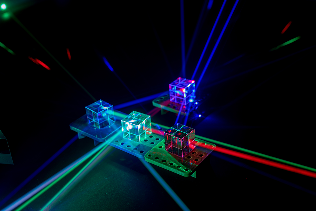
Photonics Engineers Demonstrate The Potential for Light-Based Circuits
Light-based photonics integrated circuits are thought to have the potential to transform circuits. Unlike electricity-based chips, those that use light offer faster speeds, greater bandwidth, and more energy efficiency. There’s just one problem: Currently, they’re too big.
For light-based chips, also known as photonics integrated circuits, to become effective, they need to be much smaller. They will depend on compact integration of super-fast electro-optic functional elements on a single chip that doesn’t consume too much energy.
Recently, an electrical engineering team from the University of Rochester used FEM when testing a potential solution to this problem, which they published in the August edition of Nature Communications. Using thin-film lithium niobate (LN), the team made the tiniest electro-optical modulator ever created, which they say can serve as a platform for light-based photonics integrated circuits. To do this, they bonded the lithium niobate on a silicon dioxide layer. Not only does it represent the smallest lithium niobate modulator to date, it also works at high speeds and is efficient.
“The modulators enable efficient electro-optic driving of high-Q photonic cavity modes in both adiabatic and non-adiabatic regimes, and allow us to achieve electro-optic switching at 11 Gb s−1 with a bit-switching energy as low as 22 fJ,” reported the researchers in their study. “The demonstration of energy efficient and high-speed electro-optic modulation at the wavelength scale paves a crucial foundation for realizing large-scale LN photonic integrated circuits that are of immense importance for broad applications in data communication, microwave photonics, and quantum photonics.”
Professor Qiang Lin, one of the study authors, told the University of Rochester News that lithium niobate is a “workhorse material system for photonics research and development.”
“However current LN photonic devices, made upon either bulk crystal or thin-film platform require large dimensions and are difficult to scale down in size, which limits the modulation efficiency, energy consumption, and the degree of circuit integration. A major challenge lies in making high-quality nanoscopic photonic structures with high precision,” he said.
How Else Are Photonics Researchers Using FEM?
Increasingly, researchers are using FEM to test their research. In a previous post, we discussed how researchers demonstrated off-chip beam deflection and focusing with guided wave driven metasurfaces on silicon waveguides, which has the potential to transform traditional optics technology. Like the University of Rochester team, the researchers used FEM as part of their study, showing the potential this methodology has in impacting the future of photonics.
Finite Element Method (FEM) for Photonics
This course program from IEEE Educational Activities, Finite Element Method for Photonics, provides a comprehensive and up-to-date account of FEM in photonics devices, with an emphasis on practical, problem-solving applications and real-world examples. Engineers will come away from this program with an understanding of how mathematical concepts translate to computer code finite element-based methods.
Contact an IEEE Content Specialist today to learn more about getting access to these courses for your organization.
Interested in the course for yourself? Visit the IEEE Learning Network.
Resources
Marcotte, Bob. (26 August 2020). Photonics researchers report breakthrough in miniaturizing light-based chips. University of Rochester Newscenter.
Li, Mingxiao, Ling, Jingwei, He, Yang, Javid, Usman A., Xue, Shixin & Lin, Qiang.
(17 August 2020). Lithium niobite photopic-crystal electro-optic modulator. Nature Communications.
City, University of London. 7 August 2013. City, University of London: Dr Arti Agrawal – “Finite Element Modelling for Photonics.” https://www.youtube.com/watch?v=3GNG8eKioFA
No comments yet.