
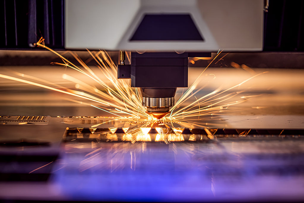
The majority of medical, scientific, and industrial applications utilize high-power diode-lasers (HPDLs). Due to the common use of HPDLs, it’s more important than ever to prevent optical and physical malfunctions in high-power laser packages. However, as laser technology has become more advanced, HPDL output power has gotten larger, and with it, the waste-heat energy density of a sole diode laser bar has expanded from 200 W/cm2 to more than 600 W/cm2.
Thermal issues often result in failures when heat gets trapped in HPDL packaging. This impacts a number of outcomes, including output power, threshold current, slope efficiency, spectral broadening, wavelength shifts, and device lifetime. However, by designing high-power laser packages using finite-element method (FEM) simulations, potential for failures can be minimized.
As discussed in a previous post, FEM is a numerical solution that breaks down a much larger, complex problem into a series of smaller ones (“finite elements”) in order to make the overall problem easier to examine. This equation is then used to create a digital simulation (known as the finite element analysis), which gives engineers a more detailed look into the design and how its various elements work together.
Using FEM to Evaluate the Thermal Performance of High-Power Diode-Lasers
Thermal stress is a major challenge when it comes to HPDLs packaging. For instance, thermal stress often leads to mechanical tension in the diode and transforms the band structure, and this changes the characteristics of the diode laser in regards to threshold, wavelength, polarization, and SMILE ( near-field nonlinearity along the laser bar). Additionally, induced thermal stress in the laser device might harm the laser chips/bars and therefore reduce the device’s lifetime.
Recently, Chinese researchers from the Design and Simulation Technology Department at Focuslight Technologies used digital simulations, including FEM, to get an up-close look at how these kinds of potential failures can be avoided.
“The finite-element model (FEM) simulation results show that the compression stress on the laser bar decreases with the increase of copper-tungsten (CuW) submount thickness, as the CuW submount works as a buffer layer and can thus absorb stress,” the researchers wrote in Laser Focus World. “However, the laser bar out-of-plane strain (SMILE value) is approximately zero when the diode-laser array is directly bonded onto the heat sink without a submount; the SMILE value is maximized when the thickness of the CuW submount is increased to 44% of the heat sink. Beyond this point, the SMILE value decreases with increasing CuW submount thickness.”
Additionally, the authors used FEM to determine that adhesion in a corner of a microlens array diffuser was the source of cracking. After they controlled the adhesion in the FEM simulation, they found they reduced stress on the diffuser.
“Easy-to-use FEM methods have been presented for evaluating the thermal performance of HPDLs and the stress distribution in HPDLs. These methods make it much easier to understand the physics of the addressed thermal phenomena and predict their thermal behavior and performance,” they wrote.
Photonics Researchers Are Increasingly Relying on FEM
More and more, photonics researchers are using FEM. In a previous post, we discussed how engineers used FEM to demonstrate the potential for light-based circuits. In another post, we discuss how researchers demonstrated off-chip beam deflection and focusing with guided wave driven metasurfaces on silicon waveguides, which has the potential to transform traditional optics technology. These are just some of the ways researchers are using FEM to revolutionize photonics.
Learn how FEM can be used to model and simulate photonic components/devices and analyze how they will behave in response to various outside influences. The Finite Element Method for Photonics course program provides a comprehensive and up-to-date account of FEM in photonics devices, with an emphasis on practical, problem-solving applications and real-world examples. Engineers will gain an understanding of how mathematical concepts translate to computer code finite element-based methods after completing this program.
Connect with an IEEE Content Specialist today to learn how to get access to this program for your organization.
Interested in the course for yourself? Visit the IEEE Learning Network (ILN).
Resources
Wang, Jingwei, Fu, Tuanwei, and Liang, Xuejie. (11 November 2020). Simulation and modeling play key roles in high-power diode-laser packaging. Laser Focus World.
[…] August, Chinese researchers from the Design and Simulation Technology Department at Focuslight Technologies used digital […]